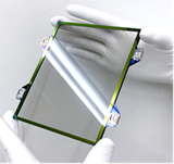
Mitsui Chemicals, Inc. (Tokyo) announced plans to set up production facilities at its Iwakuni-Ohtake Works for carbon nanotube (CNT) pellicles suited to use in next-generation high-output EUV lithography systems, which will be indispensable in further reducing the size and increasing the production efficiency of semiconductors. The new plant is expected to be completed in December 2025, with capability to produce 5,000 sheets/year.

CNT Pellicle (Source: Mitsui Chemicals)
Mitsui’s pellicle product is a dustproof photomask cover for the photolithography process, which sees semiconductor wafers exposed to light in order to etch circuit patterns. The pellicle is designed with optimal thickness to allow for high transmittance, and its membrane material is selected to provide light resistance against each exposure wavelength used. Use of pellicles keeps photomasks clean and helps improve semiconductor productivity. Since beginning pellicle sales in 1984, Mitsui Chemicals has continually strived to improve its pellicles and their quality in line with the downsizing of semiconductors.
There is particular demand growth for High NA (numerical aperture of 0.55), high-output (600W or above) lithography, which represents the next generation of EUV lithography technology. And pellicles made from new materials will be essential to withstand the harsh lithography environments required to make this technology a reality.
Mitsui Chemicals’ new mass production facilities will be a step toward commercializing CNT pellicles that have both high EUV transmittance (92% or above) and light resistance for exposure output of over 1kW. By adding next-gen pellicle products using CNT as the membrane material to its lineup alongside conventional EUV pellicles made with a silicon-based membrane, Mitsui Chemicals hopes to contribute to improved semiconductor performance and productivity.