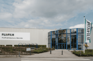
Fujifilm Corp. (Tokyo) announced that it will install new production facilities of CMP slurries, advanced semiconductor materials, and enhance existing facilities for photolithography-related materials at its production site located in Belgium. In Europe, where demand for automotive semiconductors and industrial semiconductors supporting the DX of manufacturing processes at factories is expected to grow, Fujifilm makes an investment of approximately 4 billion yen (approx. €25 million) to expand the production capacity of its Belgium site, based in Zwijndrecht, Antwerp. Operations at the site are expected to commence in the spring of 2026.

Fujifilm is making a major investment in its semiconductor business in Europe (source Fujifilm)
Driven by high-speed, high-capacity communications through 5G/6G, the expansion of autonomous driving, and the spread of AI and the metaverse, demand for semiconductors is expected to increase and their performance is projected to advance as well. Fujifilm is making proactive growth investments in the semiconductor materials business. Globally, Fujifilm plans to invest a total of 170 billion yen in growth, including research and development and capital investments, over the three years from fiscal 2024 to 2026. Fujifilm is rapidly making capital investments to expand the production capacity of semiconductor materials. The recent investment includes the enhancement of the development, production, and quality evaluation functions for advanced resists at its Shizuoka and Pyeongtaek, Korea sites, as well as the expansion of the CMP slurry production facilities at its Kumamoto site in Japan.
This time, to expand Fujifilm’s production capacity to supply the growing semiconductor market in Europe, FUJIFILM Electronic Materials (Europe) N.V., Fujifilm’s semiconductor materials subsidiary in Europe, is making a capital investment of approximately 4 billion yen (approx. 25 million EUR). It introduces new production facilities for CMP slurries, which are used in advanced semiconductors and are expected to show a high annual growth rate of 13%*3. In addition to existing CMP slurry production sites in Arizona, USA, Hsinchu and Tainan of Taiwan, Cheonan, South Korea, and Kikuyo Town, Kumamoto Prefecture, this network will be expanded by this new production capability in Belgium. This will create a global production network of six locations, ensuring a more stable supply of CMP slurries. In addition, Fujifilm will enhance the production facilities for developer used in the photolithography process at the Belgium site. This will help the company meet the increasing demand for automotive and industrial semiconductors in Europe and respond to the high-quality requirements of its customers.
The new CMP slurry production facilities and the enhanced developer production facilities are both scheduled to start operation in the spring of 2026.
Fujifilm offers semiconductor materials used in wafer processing to post processing in semiconductor manufacturing including photoresists, photolithography-related materials, CMP slurries, post-CMP cleaners, thin-film chemicals, polyimides and high-purity process chemicals, as well as WAVE CONTROL MOSAIC which includes color filter materials for image sensors. In addition to its extensive product lineup covering almost the entire range of semiconductor manufacturing processes, from leading-edge to legacy semiconductors, Fujifilm is committed to solving customers’ issues and contribute to the development of the semiconductor industry by providing one-stop solutions that leverage its global supply structure and advanced R&D capabilities.